MP-900系列beta射線鍍層測厚儀,beta射線測厚儀MP900
美國UPA beta/貝爾塔射線涂鍍層測厚儀MP-900
美國UPA Micro-Derm鍍層和涂層測厚儀MP-900
β射線反向散射測量技術
依照標準ASTM B567��,ISO/DOS 3543和DIN 50 983的準則
應用在測量許多經(jīng)典結構的鍍層厚度�,包括鎳上鍍金(Au/Ni),環(huán)氧樹脂鍍銅(Cu/epoxy)����,光致抗蝕劑photoresist,銅上鍍銀(Ag/Cu)�,科瓦鐵鈷鎳合金上鍍錫Sn/kovar,鐵上鍍氮化鈦Ti-N/Fe����,錫鉛合金Sn-Pb。
Micro-Derm MP-900可以利用霍爾效應技術測量銅上鍍鎳(Ni/Cu)的厚度。
探頭系統(tǒng)可以用于精確測量各種樣品表面����,從小零件(連接器和端子)到大零件(印制線路板)。
Micro-Derm BBS厚度標準片(4點設定)包括:純材料的底材�����,表面鍍層的純材料無限厚片和兩塊經(jīng)過NIST(美國聯(lián)邦標準技術委員會)認證的標準厚度的薄片����。
高質量的制造技術確保盡可能精確的鍍層厚度測量。
設計體現(xiàn)了無與倫比的易操作性和高效率���。
TESTING INSTRUMENTATION
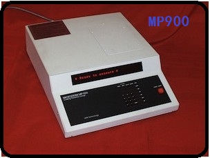
Micro-Derm MP-900
只有MP900融合了β射線反向散射和霍爾效應測量技術���。避免了因為存在兩種需要而購買了兩種儀器的麻煩。
緊湊的設計
全面的測量能力
經(jīng)濟的X射線熒光分析儀器的替代品
提高生產(chǎn)量
45種標準檔案記憶允許用戶快速的進行應用轉換�。
獨特的NOVRAM 設計使得即使在備用電源斷電時仍可以保留有價值的校準檔案。
標準校準模式:4點����,3點,2點��,線性,多點和Sn-Pb.
特殊的多點Sn-Pb校準模式可以對不同的Sn-Pb組分進行自動補償和修正��。
新的3點BBS模式并不需要純材料鍍膜標準片���。
多點校正模式應用于霍爾效應測量(測量鎳厚)���。
Micro-Derm MP-700 (已停產(chǎn))
MP700D 精確測量鍍層和涂層的厚度,例如:金���,銀,銣���,錫�����,錫鉛合金�����,銅����,鎳,光致抗蝕劑���,鋁�����,鈀和鈦鎢合金�。
可以測量任何零件
16組標準檔案存儲
因為有兩個探頭接口����,所以用戶可以方便的在兩種應用間轉換
清晰的顯示屏可以在檢測過程中不斷的提示操作者,減少錯誤
LED讀數(shù)顯示測量結果的單位可以是微英寸(microinches),微米(micrometers),毫英寸(mils)�,埃(angstroms),組分百分含量等�����。
標準特點包括自動診斷測試����,錯誤檢測,RS-232C 輸出端口
探頭�,底座和配件
PS-10A 探頭系統(tǒng)
用于測量微小零件
這種緊湊的輕量的探頭系統(tǒng)特別設計用來測量微小的電子原器件,例如:芯片(IC)���,焊盤�����,晶體管頭和導線���,扁平集成電路�����,繼電器�����,終端,針����,二極管,連接器�����,電纜等�。
型號為PS-10A的探頭應用了特大直徑的G-M管以便取得更準確的測量結果���,并且改善了統(tǒng)計功能。這種G-M管可以在鍍層測試時探測β射線反射微粒數(shù)量�����,并且將這種脈沖信號傳送給Micro-Derm主機����,在主機里這種脈沖信號被轉換成數(shù)字顯示的厚度讀數(shù)。
可互換的放射源/光圈組件
獨特的放射源環(huán)和光圈盤組件模塊確保了簡單的易更換性���,可以方便的重組大量的放射源-光圈組合����,從而可以測量幾乎所有的小零件�。
各種尺寸和型號的光圈盤配置可以方便的對測量面積進行精確限定。每種放射源和用戶指定的光圈盤一起配套成為放射源/光圈組件模組�。
光圈盤是由硬質耐磨不銹鋼制成,并且可以作成圓形或者長方形�。彈簧針將測試件牢牢固定住,暴露在光圈盤開窗下的測試件區(qū)域的鍍層厚度將被測試出來���。
光圈器固定裝置
對于難以定位的測試件�,UPA為客戶提供了光圈器固定裝置。網(wǎng)格固定裝置可以對特殊零件進行更為方便的定位����,例如焊盤,小連接器���,導線�����,等�����。這種完整的組件是由零件固定器設備和配套的精確光圈盤組成��。
CB-5型底座
專門用于印制線路板測試
這種新專利的線路板型CB-5底座���,可以為在印制線路板上的表面鍍層厚度進行出乎意外的快速和精確測量�����。
通過這種獨特的光學定位系統(tǒng)���,CB-5就可以方便地將HH-3測試探頭(見上頁)定位在線路板上的微小區(qū)域內���。將CB-5放置在線路板上��,線路板上的被檢測點將被照亮��,并不需要類似十字準線式的對準方法進行對準����。
既然CB-5底座可以移動到線路板上的任何位置���,那么它就可以對即使處于特大型線路板的中心位置這樣類似難以檢測的區(qū)域進行測試����。通過利用C-3卡子和HH-3探頭系統(tǒng)就可以快速的對放置在CB-5中的探頭進行更換��。
Micro-Derm探頭和底座
HH-3探頭
一套獨立的探頭系統(tǒng)包括一個盛裝β射線放射源(Pm,Tl,Sr)的探頭桶MB-3,一個Geiger-MullerG-M管����,一個樣品罩。
這種多樣化的探頭可以和多種探頭底座和支架相配套�����,從而可以確保對各種尺寸和形狀的零件進行測量,例如線路板����,圓柱,制罐用薄板材料�,平板,底盤�,小零件。
HH-4探頭
這種緊湊的獨立的探頭系統(tǒng)確?�?梢詼y量直徑小至0.5"12.7mm內曲面或內
平面的激光視盤�����。這種獨特的配置可以使β射線微粒從探頭側面開窗發(fā)射出來����。可以測量軸承��、環(huán)狀物�����、管子����、波導、圓柱等內側表面的金�����、銠�����、銀�����、石墨��、錫鉛合金以及其它鍍層的厚度�。
TR-1探頭系統(tǒng)
這種探頭用于測量高密硬盤,金屬薄片���,膠帶��,硅晶片��,等�����。用探頭TR-1把樣品放置在β射線放射源和G-M管探測器之間進行測量是非接觸的�����,這樣就允許不斷的移動金屬薄片和膠帶進行測量����,需要配置Tl放射源。
TR-1探頭系統(tǒng)提供非接觸的測量��。
小零件探頭底座SPG-1
這種底座用于定位HH-3探頭對小型電子零件進行測量��,比如連接器���,針頭���,焊盤,電線��,扁平集成電路和接觸端���。樣品固定壓力針可以安全的固定樣品����。這種底座可以確保同樣的標準HH-3探頭既可以用于測量有巨大的表面的零件���,也可以測量小型零部件���。
我們專業(yè)的應用工程師將很高興為適應您的特殊的測量應用的需要而配置挑選合適的零部件。
座臺式:
Microderm MP-900
Beta Backscatter and Hall Effect System!
Microderm MP-900
For companies that prefer a benchtop model
- Measures many typical thickness applications, including gold on nickel, copper on epoxy, photoresist, silver on copper, tin on kovar, titanium nitrate on steel, tin-lead alloys
- Microderm Beta Backscatter thickness standards (4 point sets) consist of a bare sample of base material, a sample of infinitely thick coating material, and two thickness standards certified traceable to the NIST (National Institute of Standards Technology)
- Can measure nickel thickness on copper using the Hall effect
- Each measurement system comes complete with a benchtop measuring instrument, a measuring probe and guide, and thickness standards
- Designed for unmatched ease-of-use and efficiency
Probes
All Microderm probes work with either the handheld or benchtop model
HH3 Probe
- Self contained probe system consisting of a probe barrel, beta source, Geiger-Muller tube sensor, specimen mask, and case assembly.
- Can be used with any of several probe guides and stands, enabling measurement on almost any size or shape of part.
WF Probe Guide
- The WF probe guide is used with the HH-3 or HH-2 probe and attaches in seconds without tools.
- This handy probe guide is balanced with a metal outer ring, which encircles a polished Lucite core.
- The guide holds the probe steady on horizontal surfaces.
SPG-1 Small Parts Probe Guide
- Uses an HH-3 probe and attaches in seconds without tools.
- A spring-mounted pressure pin holds small parts securely on the HH-3 probe for accurate, repeatable measurements.
The PS-10A Probe Table
- Allows precise, instant alignment of very small parts. Electronic components such as connectors, contacts, pins, and terminals are readily measured with the probe system
- A spring-loaded pressure pin securely hold parts steady.
Beta Thin Films "BTF" Probe
- Measures wet or dry coatings such as stamping lubricants, primers and adhesives on flat parts.
- Extremely thin organic and metal film coatings are accurately measured
手持式:
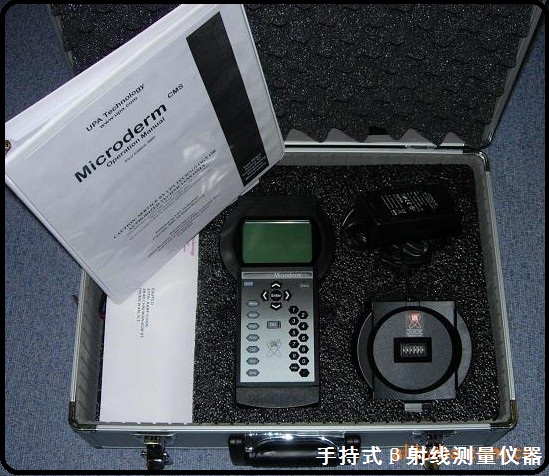
Microderm CMS, Benchtop, and Probes
Microderm CMS
The World‘s First Portable BetaBackscatter Device
The UPA Microderm CMS is a handheld unit perfect for process-line operation. Its menu-driven interactive software and re-charging docking station with spare battery pack makes it versatile and easy to use. It offers a data management software with 100 applications, 40 calibrations, and 10,000 measurements. Statistics include mean, standard deviation, highest/lowest measurement, and range.
- A wide variety of probes and probe stands allows measurement on almost any size or shape of part
- Menu-driven, user-friendly software, and an easy-to-read backlit display
- Ergonomic instrument design for unmatched ease of use and efficiency
- Rechargeable NiMH batteries provide up to 20 hours of continuous measuring between recharges
- Recharging base also functions as a benchtop stand
- Calibrates in minutes using NIST traceable standards
|
MicrodermCMSSpecifications:
|
|
Dimensions
|
9.5" X 5.0" X 2.5" (250 mm x 125 mm x 62.5 cm)
|
|
Weight
|
1.5 lbs. (0.65 kg)
|
|
Display
|
2" X 2.4" (50mm x 60mm) backlit viewing area 320 x 240 pixels; 1/4 VGA
|
|
Memory
|
100 applications; 20 calibrations; 350,000 measurement storage
|
|
Statistics
|
Mean, standard deviation, max/min, and range
|
|
Data Port
|
9-Pin Serial to USB
|
|
Batteries
|
Rechargeable, NiMH batteries
|
Typical Applications Include
- Adhesive / Steel, Aluminum, Glass
- Aluminum / Kovar, Steel, Glass, Silicon
- Aluminide / Nickel Alloys
- Babbitt / Bronze, Brass, Copper, Iron
- Copper / Aluminum, Beryllium, Carbon, Ceramic, Plastic
- Chromium / Copper, Aluminum
- Cadmium / Steel, Brass, Stainless Steel
- Electroless Nickel / Aluminum, Plastic
- Gold / Nickel, Copper, Silicon, Ceramic
- Iron Oxide / Mylar
|
- Lead / Brass, Bronze
- Lubricants / Steel, Aluminum, Brass, Copper
- Mylar Film Thickness
- Nickel / Aluminum, Beryllium
- Palladium / Nickel
- PhotoResist / Copper
- Platinum / Nickel
- Primer / Glass
- Rhodium / Nickel, Copper, Gold
- Silver / Copper, Nickel, Ceramic
- Silicon / Plastic
- Solder / Copper, Brass
- Tantalum / Glass
- Tin / Copper, Brass, Steel
- Tin-Nickel / Nickel
- Titanium Nitride / Steel, Stainless Steel
|
Microderm Technology is also used for the precise measurement of stamping lubricants
- No additives are necessary for measuring lubricants
- Measures lubricants on any metal substrate
- All lubricants are measured using a single calibration
- Independent testing confirms correlation to weigh/strip/weigh
- Used by Toyota, Ford, Chrysler, and Nissan
MP-900系列beta射線鍍層測厚儀,beta射線測厚儀MP900
美國UPA beta/貝爾塔射線涂鍍層測厚儀MP-900
美國UPA Micro-Derm鍍層和涂層測厚儀MP-900
β射線反向散射測量技術
依照標準ASTM B567��,ISO/DOS 3543和DIN 50 983的準則
應用在測量許多經(jīng)典結構的鍍層厚度�,包括鎳上鍍金(Au/Ni),環(huán)氧樹脂鍍銅(Cu/epoxy),光致抗蝕劑photoresist���,銅上鍍銀(Ag/Cu)�����,科瓦鐵鈷鎳合金上鍍錫Sn/kovar�����,鐵上鍍氮化鈦Ti-N/Fe�����,錫鉛合金Sn-Pb�。
Micro-Derm MP-900可以利用霍爾效應技術測量銅上鍍鎳(Ni/Cu)的厚度。
探頭系統(tǒng)可以用于精確測量各種樣品表面���,從小零件(連接器和端子)到大零件(印制線路板)�。
Micro-Derm BBS厚度標準片(4點設定)包括:純材料的底材���,表面鍍層的純材料無限厚片和兩塊經(jīng)過NIST(美國聯(lián)邦標準技術委員會)認證的標準厚度的薄片���。
高質量的制造技術確保盡可能精確的鍍層厚度測量。
設計體現(xiàn)了無與倫比的易操作性和高效率�。
TESTING INSTRUMENTATION
Micro-Derm MP-900
只有MP900融合了β射線反向散射和霍爾效應測量技術。避免了因為存在兩種需要而購買了兩種儀器的麻煩�����。
緊湊的設計
全面的測量能力
經(jīng)濟的X射線熒光分析儀器的替代品
提高生產(chǎn)量
45種標準檔案記憶允許用戶快速的進行應用轉換��。
獨特的NOVRAM 設計使得即使在備用電源斷電時仍可以保留有價值的校準檔案�����。
標準校準模式:4點,3點����,2點,線性�����,多點和Sn-Pb.
特殊的多點Sn-Pb校準模式可以對不同的Sn-Pb組分進行自動補償和修正�����。
新的3點BBS模式并不需要純材料鍍膜標準片��。
多點校正模式應用于霍爾效應測量(測量鎳厚)�。
Micro-Derm MP-700 (已停產(chǎn))
MP700D 精確測量鍍層和涂層的厚度�����,例如:金���,銀�����,銣���,錫���,錫鉛合金,銅��,鎳����,光致抗蝕劑,鋁�����,鈀和鈦鎢合金�����。
可以測量任何零件
16組標準檔案存儲
因為有兩個探頭接口��,所以用戶可以方便的在兩種應用間轉換
清晰的顯示屏可以在檢測過程中不斷的提示操作者���,減少錯誤
LED讀數(shù)顯示測量結果的單位可以是微英寸(microinches),微米(micrometers),毫英寸(mils)���,埃(angstroms)�,組分百分含量等�����。
標準特點包括自動診斷測試��,錯誤檢測����,RS-232C 輸出端口
探頭����,底座和配件
PS-10A 探頭系統(tǒng)
用于測量微小零件
這種緊湊的輕量的探頭系統(tǒng)特別設計用來測量微小的電子原器件,例如:芯片(IC)��,焊盤����,晶體管頭和導線,扁平集成電路���,繼電器�,終端,針�,二極管,連接器��,電纜等�。
型號為PS-10A的探頭應用了特大直徑的G-M管以便取得更準確的測量結果,并且改善了統(tǒng)計功能����。這種G-M管可以在鍍層測試時探測β射線反射微粒數(shù)量,并且將這種脈沖信號傳送給Micro-Derm主機���,在主機里這種脈沖信號被轉換成數(shù)字顯示的厚度讀數(shù)�。
可互換的放射源/光圈組件
獨特的放射源環(huán)和光圈盤組件模塊確保了簡單的易更換性��,可以方便的重組大量的放射源-光圈組合��,從而可以測量幾乎所有的小零件�。
各種尺寸和型號的光圈盤配置可以方便的對測量面積進行精確限定。每種放射源和用戶指定的光圈盤一起配套成為放射源/光圈組件模組�����。
光圈盤是由硬質耐磨不銹鋼制成,并且可以作成圓形或者長方形�����。彈簧針將測試件牢牢固定住��,暴露在光圈盤開窗下的測試件區(qū)域的鍍層厚度將被測試出來�。
光圈器固定裝置
對于難以定位的測試件,UPA為客戶提供了光圈器固定裝置����。網(wǎng)格固定裝置可以對特殊零件進行更為方便的定位,例如焊盤�����,小連接器����,導線�,等。這種完整的組件是由零件固定器設備和配套的精確光圈盤組成�。
CB-5型底座
專門用于印制線路板測試
這種新專利的線路板型CB-5底座,可以為在印制線路板上的表面鍍層厚度進行出乎意外的快速和精確測量��。
通過這種獨特的光學定位系統(tǒng)�,CB-5就可以方便地將HH-3測試探頭(見上頁)定位在線路板上的微小區(qū)域內�����。將CB-5放置在線路板上���,線路板上的被檢測點將被照亮,并不需要類似十字準線式的對準方法進行對準��。
既然CB-5底座可以移動到線路板上的任何位置����,那么它就可以對即使處于特大型線路板的中心位置這樣類似難以檢測的區(qū)域進行測試。通過利用C-3卡子和HH-3探頭系統(tǒng)就可以快速的對放置在CB-5中的探頭進行更換����。
Micro-Derm探頭和底座
HH-3探頭
一套獨立的探頭系統(tǒng)包括一個盛裝β射線放射源(Pm,Tl,Sr)的探頭桶MB-3,一個Geiger-MullerG-M管,一個樣品罩�。
這種多樣化的探頭可以和多種探頭底座和支架相配套,從而可以確保對各種尺寸和形狀的零件進行測量�,例如線路板,圓柱����,制罐用薄板材料,平板,底盤�����,小零件���。
HH-4探頭
這種緊湊的獨立的探頭系統(tǒng)確?����?梢詼y量直徑小至0.5"12.7mm內曲面或內
平面的激光視盤��。這種獨特的配置可以使β射線微粒從探頭側面開窗發(fā)射出來�����?��?梢詼y量軸承、環(huán)狀物�、管子��、波導�����、圓柱等內側表面的金、銠����、銀、石墨��、錫鉛合金以及其它鍍層的厚度��。
TR-1探頭系統(tǒng)
這種探頭用于測量高密硬盤��,金屬薄片��,膠帶���,硅晶片��,等��。用探頭TR-1把樣品放置在β射線放射源和G-M管探測器之間進行測量是非接觸的��,這樣就允許不斷的移動金屬薄片和膠帶進行測量��,需要配置Tl放射源��。
TR-1探頭系統(tǒng)提供非接觸的測量��。
小零件探頭底座SPG-1
這種底座用于定位HH-3探頭對小型電子零件進行測量�����,比如連接器���,針頭����,焊盤���,電線���,扁平集成電路和接觸端。樣品固定壓力針可以安全的固定樣品���。這種底座可以確保同樣的標準HH-3探頭既可以用于測量有巨大的表面的零件�����,也可以測量小型零部件�����。
我們專業(yè)的應用工程師將很高興為適應您的特殊的測量應用的需要而配置挑選合適的零部件��。
座臺式:
Microderm MP-900
Beta Backscatter and Hall Effect System!
Microderm MP-900
For companies that prefer a benchtop model
- Measures many typical thickness applications, including gold on nickel, copper on epoxy, photoresist, silver on copper, tin on kovar, titanium nitrate on steel, tin-lead alloys
- Microderm Beta Backscatter thickness standards (4 point sets) consist of a bare sample of base material, a sample of infinitely thick coating material, and two thickness standards certified traceable to the NIST (National Institute of Standards Technology)
- Can measure nickel thickness on copper using the Hall effect
- Each measurement system comes complete with a benchtop measuring instrument, a measuring probe and guide, and thickness standards
- Designed for unmatched ease-of-use and efficiency
Probes
All Microderm probes work with either the handheld or benchtop model
HH3 Probe
- Self contained probe system consisting of a probe barrel, beta source, Geiger-Muller tube sensor, specimen mask, and case assembly.
- Can be used with any of several probe guides and stands, enabling measurement on almost any size or shape of part.
WF Probe Guide
- The WF probe guide is used with the HH-3 or HH-2 probe and attaches in seconds without tools.
- This handy probe guide is balanced with a metal outer ring, which encircles a polished Lucite core.
- The guide holds the probe steady on horizontal surfaces.
SPG-1 Small Parts Probe Guide
- Uses an HH-3 probe and attaches in seconds without tools.
- A spring-mounted pressure pin holds small parts securely on the HH-3 probe for accurate, repeatable measurements.
The PS-10A Probe Table
- Allows precise, instant alignment of very small parts. Electronic components such as connectors, contacts, pins, and terminals are readily measured with the probe system
- A spring-loaded pressure pin securely hold parts steady.
Beta Thin Films "BTF" Probe
- Measures wet or dry coatings such as stamping lubricants, primers and adhesives on flat parts.
- Extremely thin organic and metal film coatings are accurately measured
手持式:
Microderm CMS, Benchtop, and Probes
Microderm CMS
The World‘s First Portable BetaBackscatter Device
The UPA Microderm CMS is a handheld unit perfect for process-line operation. Its menu-driven interactive software and re-charging docking station with spare battery pack makes it versatile and easy to use. It offers a data management software with 100 applications, 40 calibrations, and 10,000 measurements. Statistics include mean, standard deviation, highest/lowest measurement, and range.
- A wide variety of probes and probe stands allows measurement on almost any size or shape of part
- Menu-driven, user-friendly software, and an easy-to-read backlit display
- Ergonomic instrument design for unmatched ease of use and efficiency
- Rechargeable NiMH batteries provide up to 20 hours of continuous measuring between recharges
- Recharging base also functions as a benchtop stand
- Calibrates in minutes using NIST traceable standards
|
MicrodermCMSSpecifications:
|
|
Dimensions
|
9.5" X 5.0" X 2.5" (250 mm x 125 mm x 62.5 cm)
|
|
Weight
|
1.5 lbs. (0.65 kg)
|
|
Display
|
2" X 2.4" (50mm x 60mm) backlit viewing area 320 x 240 pixels; 1/4 VGA
|
|
Memory
|
100 applications; 20 calibrations; 350,000 measurement storage
|
|
Statistics
|
Mean, standard deviation, max/min, and range
|
|
Data Port
|
9-Pin Serial to USB
|
|
Batteries
|
Rechargeable, NiMH batteries
|
Typical Applications Include
- Adhesive / Steel, Aluminum, Glass
- Aluminum / Kovar, Steel, Glass, Silicon
- Aluminide / Nickel Alloys
- Babbitt / Bronze, Brass, Copper, Iron
- Copper / Aluminum, Beryllium, Carbon, Ceramic, Plastic
- Chromium / Copper, Aluminum
- Cadmium / Steel, Brass, Stainless Steel
- Electroless Nickel / Aluminum, Plastic
- Gold / Nickel, Copper, Silicon, Ceramic
- Iron Oxide / Mylar
|
- Lead / Brass, Bronze
- Lubricants / Steel, Aluminum, Brass, Copper
- Mylar Film Thickness
- Nickel / Aluminum, Beryllium
- Palladium / Nickel
- PhotoResist / Copper
- Platinum / Nickel
- Primer / Glass
- Rhodium / Nickel, Copper, Gold
- Silver / Copper, Nickel, Ceramic
- Silicon / Plastic
- Solder / Copper, Brass
- Tantalum / Glass
- Tin / Copper, Brass, Steel
- Tin-Nickel / Nickel
- Titanium Nitride / Steel, Stainless Steel
|
Microderm Technology is also used for the precise measurement of stamping lubricants
- No additives are necessary for measuring lubricants
- Measures lubricants on any metal substrate
- All lubricants are measured using a single calibration
- Independent testing confirms correlation to weigh/strip/weigh
- Used by Toyota, Ford, Chrysler, and Nissan
MP-900系列beta射線鍍層測厚儀,beta射線測厚儀MP900
美國UPA beta/貝爾塔射線涂鍍層測厚儀MP-900
美國UPA Micro-Derm鍍層和涂層測厚儀MP-900
β射線反向散射測量技術
依照標準ASTM B567�����,ISO/DOS 3543和DIN 50 983的準則
應用在測量許多經(jīng)典結構的鍍層厚度����,包括鎳上鍍金(Au/Ni),環(huán)氧樹脂鍍銅(Cu/epoxy)�,光致抗蝕劑photoresist,銅上鍍銀(Ag/Cu)�,科瓦鐵鈷鎳合金上鍍錫Sn/kovar,鐵上鍍氮化鈦Ti-N/Fe����,錫鉛合金Sn-Pb。
Micro-Derm MP-900可以利用霍爾效應技術測量銅上鍍鎳(Ni/Cu)的厚度���。
探頭系統(tǒng)可以用于精確測量各種樣品表面����,從小零件(連接器和端子)到大零件(印制線路板)。
Micro-Derm BBS厚度標準片(4點設定)包括:純材料的底材���,表面鍍層的純材料無限厚片和兩塊經(jīng)過NIST(美國聯(lián)邦標準技術委員會)認證的標準厚度的薄片�����。
高質量的制造技術確保盡可能精確的鍍層厚度測量���。
設計體現(xiàn)了無與倫比的易操作性和高效率。
TESTING INSTRUMENTATION
Micro-Derm MP-900
只有MP900融合了β射線反向散射和霍爾效應測量技術��。避免了因為存在兩種需要而購買了兩種儀器的麻煩���。
緊湊的設計
全面的測量能力
經(jīng)濟的X射線熒光分析儀器的替代品
提高生產(chǎn)量
45種標準檔案記憶允許用戶快速的進行應用轉換��。
獨特的NOVRAM 設計使得即使在備用電源斷電時仍可以保留有價值的校準檔案���。
標準校準模式:4點,3點����,2點,線性�����,多點和Sn-Pb.
特殊的多點Sn-Pb校準模式可以對不同的Sn-Pb組分進行自動補償和修正。
新的3點BBS模式并不需要純材料鍍膜標準片����。
多點校正模式應用于霍爾效應測量(測量鎳厚)�。
Micro-Derm MP-700 (已停產(chǎn))
MP700D 精確測量鍍層和涂層的厚度,例如:金��,銀�,銣,錫��,錫鉛合金�,銅,鎳�����,光致抗蝕劑�,鋁,鈀和鈦鎢合金��。
可以測量任何零件
16組標準檔案存儲
因為有兩個探頭接口�����,所以用戶可以方便的在兩種應用間轉換
清晰的顯示屏可以在檢測過程中不斷的提示操作者,減少錯誤
LED讀數(shù)顯示測量結果的單位可以是微英寸(microinches),微米(micrometers),毫英寸(mils)����,埃(angstroms),組分百分含量等����。
標準特點包括自動診斷測試,錯誤檢測���,RS-232C 輸出端口
探頭�,底座和配件
PS-10A 探頭系統(tǒng)
用于測量微小零件
這種緊湊的輕量的探頭系統(tǒng)特別設計用來測量微小的電子原器件���,例如:芯片(IC)��,焊盤����,晶體管頭和導線���,扁平集成電路���,繼電器��,終端����,針�,二極管���,連接器�,電纜等�。
型號為PS-10A的探頭應用了特大直徑的G-M管以便取得更準確的測量結果����,并且改善了統(tǒng)計功能����。這種G-M管可以在鍍層測試時探測β射線反射微粒數(shù)量,并且將這種脈沖信號傳送給Micro-Derm主機���,在主機里這種脈沖信號被轉換成數(shù)字顯示的厚度讀數(shù)����。
可互換的放射源/光圈組件
獨特的放射源環(huán)和光圈盤組件模塊確保了簡單的易更換性,可以方便的重組大量的放射源-光圈組合�����,從而可以測量幾乎所有的小零件���。
各種尺寸和型號的光圈盤配置可以方便的對測量面積進行精確限定���。每種放射源和用戶指定的光圈盤一起配套成為放射源/光圈組件模組。
光圈盤是由硬質耐磨不銹鋼制成�,并且可以作成圓形或者長方形。彈簧針將測試件牢牢固定住���,暴露在光圈盤開窗下的測試件區(qū)域的鍍層厚度將被測試出來����。
光圈器固定裝置
對于難以定位的測試件�,UPA為客戶提供了光圈器固定裝置。網(wǎng)格固定裝置可以對特殊零件進行更為方便的定位����,例如焊盤,小連接器,導線����,等。這種完整的組件是由零件固定器設備和配套的精確光圈盤組成�����。
CB-5型底座
專門用于印制線路板測試
這種新專利的線路板型CB-5底座�,可以為在印制線路板上的表面鍍層厚度進行出乎意外的快速和精確測量。
通過這種獨特的光學定位系統(tǒng)�����,CB-5就可以方便地將HH-3測試探頭(見上頁)定位在線路板上的微小區(qū)域內��。將CB-5放置在線路板上����,線路板上的被檢測點將被照亮����,并不需要類似十字準線式的對準方法進行對準。
既然CB-5底座可以移動到線路板上的任何位置�,那么它就可以對即使處于特大型線路板的中心位置這樣類似難以檢測的區(qū)域進行測試。通過利用C-3卡子和HH-3探頭系統(tǒng)就可以快速的對放置在CB-5中的探頭進行更換。
Micro-Derm探頭和底座
HH-3探頭
一套獨立的探頭系統(tǒng)包括一個盛裝β射線放射源(Pm,Tl,Sr)的探頭桶MB-3,一個Geiger-MullerG-M管��,一個樣品罩�。
這種多樣化的探頭可以和多種探頭底座和支架相配套,從而可以確保對各種尺寸和形狀的零件進行測量����,例如線路板,圓柱�����,制罐用薄板材料�,平板,底盤����,小零件。
HH-4探頭
這種緊湊的獨立的探頭系統(tǒng)確?���?梢詼y量直徑小至0.5"12.7mm內曲面或內
平面的激光視盤。這種獨特的配置可以使β射線微粒從探頭側面開窗發(fā)射出來�����。可以測量軸承��、環(huán)狀物�����、管子����、波導、圓柱等內側表面的金����、銠、銀�、石墨、錫鉛合金以及其它鍍層的厚度����。
TR-1探頭系統(tǒng)
這種探頭用于測量高密硬盤���,金屬薄片���,膠帶�����,硅晶片�����,等�����。用探頭TR-1把樣品放置在β射線放射源和G-M管探測器之間進行測量是非接觸的�����,這樣就允許不斷的移動金屬薄片和膠帶進行測量�����,需要配置Tl放射源����。
TR-1探頭系統(tǒng)提供非接觸的測量����。
小零件探頭底座SPG-1
這種底座用于定位HH-3探頭對小型電子零件進行測量��,比如連接器���,針頭,焊盤���,電線���,扁平集成電路和接觸端。樣品固定壓力針可以安全的固定樣品�。這種底座可以確保同樣的標準HH-3探頭既可以用于測量有巨大的表面的零件,也可以測量小型零部件���。
我們專業(yè)的應用工程師將很高興為適應您的特殊的測量應用的需要而配置挑選合適的零部件�。
座臺式:
Microderm MP-900
Beta Backscatter and Hall Effect System!
Microderm MP-900
For companies that prefer a benchtop model
- Measures many typical thickness applications, including gold on nickel, copper on epoxy, photoresist, silver on copper, tin on kovar, titanium nitrate on steel, tin-lead alloys
- Microderm Beta Backscatter thickness standards (4 point sets) consist of a bare sample of base material, a sample of infinitely thick coating material, and two thickness standards certified traceable to the NIST (National Institute of Standards Technology)
- Can measure nickel thickness on copper using the Hall effect
- Each measurement system comes complete with a benchtop measuring instrument, a measuring probe and guide, and thickness standards
- Designed for unmatched ease-of-use and efficiency
Probes
All Microderm probes work with either the handheld or benchtop model
HH3 Probe
- Self contained probe system consisting of a probe barrel, beta source, Geiger-Muller tube sensor, specimen mask, and case assembly.
- Can be used with any of several probe guides and stands, enabling measurement on almost any size or shape of part.
WF Probe Guide
- The WF probe guide is used with the HH-3 or HH-2 probe and attaches in seconds without tools.
- This handy probe guide is balanced with a metal outer ring, which encircles a polished Lucite core.
- The guide holds the probe steady on horizontal surfaces.
SPG-1 Small Parts Probe Guide
- Uses an HH-3 probe and attaches in seconds without tools.
- A spring-mounted pressure pin holds small parts securely on the HH-3 probe for accurate, repeatable measurements.
The PS-10A Probe Table
- Allows precise, instant alignment of very small parts. Electronic components such as connectors, contacts, pins, and terminals are readily measured with the probe system
- A spring-loaded pressure pin securely hold parts steady.
Beta Thin Films "BTF" Probe
- Measures wet or dry coatings such as stamping lubricants, primers and adhesives on flat parts.
- Extremely thin organic and metal film coatings are accurately measured
手持式:
Microderm CMS, Benchtop, and Probes
Microderm CMS
The World‘s First Portable BetaBackscatter Device
The UPA Microderm CMS is a handheld unit perfect for process-line operation. Its menu-driven interactive software and re-charging docking station with spare battery pack makes it versatile and easy to use. It offers a data management software with 100 applications, 40 calibrations, and 10,000 measurements. Statistics include mean, standard deviation, highest/lowest measurement, and range.
- A wide variety of probes and probe stands allows measurement on almost any size or shape of part
- Menu-driven, user-friendly software, and an easy-to-read backlit display
- Ergonomic instrument design for unmatched ease of use and efficiency
- Rechargeable NiMH batteries provide up to 20 hours of continuous measuring between recharges
- Recharging base also functions as a benchtop stand
- Calibrates in minutes using NIST traceable standards
|
MicrodermCMSSpecifications:
|
|
Dimensions
|
9.5" X 5.0" X 2.5" (250 mm x 125 mm x 62.5 cm)
|
|
Weight
|
1.5 lbs. (0.65 kg)
|
|
Display
|
2" X 2.4" (50mm x 60mm) backlit viewing area 320 x 240 pixels; 1/4 VGA
|
|
Memory
|
100 applications; 20 calibrations; 350,000 measurement storage
|
|
Statistics
|
Mean, standard deviation, max/min, and range
|
|
Data Port
|
9-Pin Serial to USB
|
|
Batteries
|
Rechargeable, NiMH batteries
|
Typical Applications Include
- Adhesive / Steel, Aluminum, Glass
- Aluminum / Kovar, Steel, Glass, Silicon
- Aluminide / Nickel Alloys
- Babbitt / Bronze, Brass, Copper, Iron
- Copper / Aluminum, Beryllium, Carbon, Ceramic, Plastic
- Chromium / Copper, Aluminum
- Cadmium / Steel, Brass, Stainless Steel
- Electroless Nickel / Aluminum, Plastic
- Gold / Nickel, Copper, Silicon, Ceramic
- Iron Oxide / Mylar
|
- Lead / Brass, Bronze
- Lubricants / Steel, Aluminum, Brass, Copper
- Mylar Film Thickness
- Nickel / Aluminum, Beryllium
- Palladium / Nickel
- PhotoResist / Copper
- Platinum / Nickel
- Primer / Glass
- Rhodium / Nickel, Copper, Gold
- Silver / Copper, Nickel, Ceramic
- Silicon / Plastic
- Solder / Copper, Brass
- Tantalum / Glass
- Tin / Copper, Brass, Steel
- Tin-Nickel / Nickel
- Titanium Nitride / Steel, Stainless Steel
|
Microderm Technology is also used for the precise measurement of stamping lubricants
- No additives are necessary for measuring lubricants
- Measures lubricants on any metal substrate
- All lubricants are measured using a single calibration
- Independent testing confirms correlation to weigh/strip/weigh
- Used by Toyota, Ford, Chrysler, and Nissan

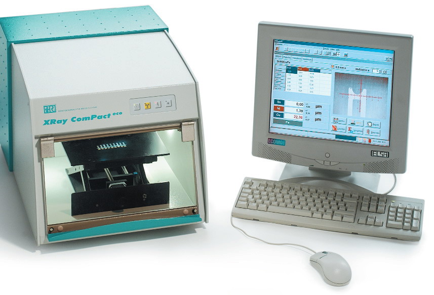
Xray Compact eco
$Xray Compact eco
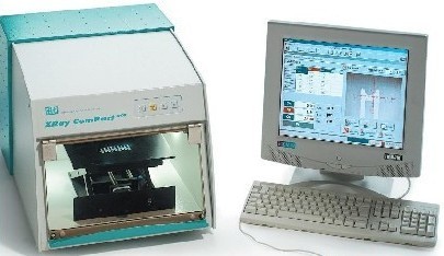
德國金屬鍍層測厚儀Compact eco
$Compact eco
CMI243金屬鍍層測厚儀
$CMI200/CMI243
beta射線測厚儀MP900
$MP900/HH3/WF/BTF/SPG-1
汽車玻璃表面油膜厚度測量儀CMS
$玻璃表面油膜厚度測量儀

CMS beta射線測厚儀
$CMS beta射線測厚儀
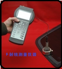
手持式β射線測量儀器CMS
$CMS
金屬鍍層測厚儀compacteco
$Roentgenanalytik

X射線熒光分析儀compact eco
$compact eco